C-PHY and D-PHY routing on Jetson Orin custom carrier boards, hardware design guide
MIPI CSI-2 routing failures on custom carrier boards almost never show up in electrical tests, the traces look fine on a VNA, the signal looks clean on a differential probe, and yet the camera driver won’t lock or produces intermittent errors. The failure mode is almost always a combination of lane length mismatch, via discontinuities, and stacked-up impedance errors that only manifest at the 1–2.5Gbps data rates used in production.
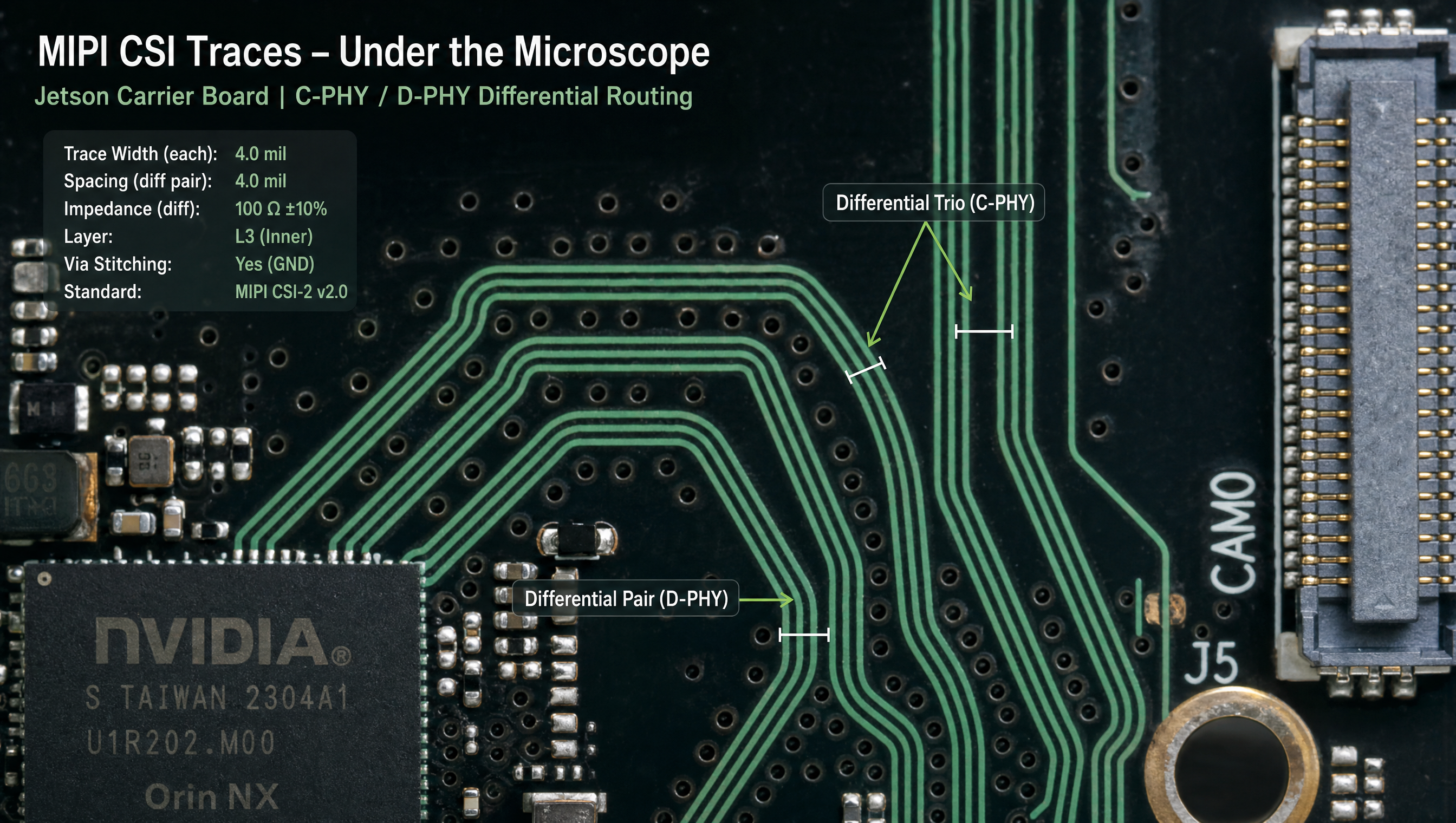
Key Insights
- Length matching is more critical than absolute trace length: intra-pair skew (between + and - of a differential pair) must be < 5mm; inter-lane skew (between data lanes) must be < 10mm
- Vias destroy impedance continuity: each via adds 0.5–1pF capacitance; minimize vias on MIPI lanes, and back-drill or use microvia stacks if vias are unavoidable
- Reference plane continuity matters: do not route MIPI traces over split or interrupted ground planes; every gap in the reference plane causes a localized impedance change
- C-PHY requires symmetrical 3-conductor routing: all three conductors in a trio must be identical in length and impedance; asymmetry degrades the eye opening
- The Jetson module connector defines the impedance reference: traces must maintain 100Ω differential from the module connector to the camera connector with no discontinuities
D-PHY lane structure
Jetson Orin Module
(CSI0, 4 lanes)
  │
  ├── CLK_P / CLK_N    (clock lane, differential pair)
  ├── DATA0_P / DATA0_N (data lane 0)
  ├── DATA1_P / DATA1_N (data lane 1)
  ├── DATA2_P / DATA2_N (data lane 2)
  └── DATA3_P / DATA3_N (data lane 3)
         │
         │  ← PCB traces (must maintain 100Ω differential)
         │
  Camera connector / flex
C-PHY trio structure
Jetson Orin Module
(CSI0, 3 trios = 6 lanes equivalent)
  │
  ├── TRIO0_A / TRIO0_B / TRIO0_C   (3 conductors per trio)
  ├── TRIO1_A / TRIO1_B / TRIO1_C
  └── TRIO2_A / TRIO2_B / TRIO2_C
         │
         │  ← PCB traces (60Ω single-ended each conductor)
         │
  Camera connector
PCB stackup recommendation
For a 4-layer carrier board carrying MIPI signals:
Layer 1: Signal (MIPI traces, component side)
Layer 2: Ground plane (continuous, no splits under MIPI)
Layer 3: Power planes (split OK, away from MIPI)
Layer 4: Signal (other signals, opposite side)
Target trace parameters (FR4, 4-layer, 1oz copper):
- Trace width: 0.1mm (4 mil)
- Trace spacing: 0.1mm intra-pair, 0.3mm inter-pair
- Differential impedance: 100Ω ± 10%
For 6-layer boards with blind/buried vias (recommended for multi-CSI carrier boards):
Layer 1: Signal (MIPI)
Layer 2: Ground
Layer 3: Signal (other)
Layer 4: Ground
Layer 5: Power
Layer 6: Signal (other)
Length matching rules
| Constraint | Required tolerance | Notes |
|---|---|---|
| Intra-pair (P vs N) | < 5mm | Use serpentine near the connector |
| Inter-lane (DATA0 vs DATA1 vs …) | < 10mm | Clock and data can differ more |
| Clock vs data (D-PHY) | < 20mm | Clock is recovered separately |
| C-PHY trio conductors (A, B, C) | < 2mm | Tighter than D-PHY due to trio encoding |
Good: serpentine length-matching on the P trace to match N
┌──────────────────────────────────────────────────┐
│  DATA0_P: ─────────────────────────────────────  │
│  DATA0_N: ─────┬──┬───────────────────────────  │
│                └──┘ (serpentine adds ~3mm)        │
└──────────────────────────────────────────────────┘

Bad: sharp bends on differential pairs
DATA0_P: ───────┐     (adds stub and impedance change)
                └──────
DATA0_N: ─────────────
Via minimization
Each via on a MIPI lane adds capacitance that causes a local impedance dip. At 2.5Gbps:
- 0 vias: minimal signal degradation
- 1 via per lane: ~0.5–1% reflections (usually acceptable)
- 2+ vias per lane: significant eye closure, increased BER
If vias are unavoidable:
- Use microvia stacks (buried/blind) instead of through-hole vias, smaller capacitance
- Back-drill through-hole vias to remove the stub below the exit layer
- Place vias in pairs (one on P, one on N at the same location) to maintain pair balance
Connector selection
| Connector type | Max data rate | Notes |
|---|---|---|
| Molex FPC 0.5mm pitch | 2.5Gbps/lane | Standard for sensor flex connections |
| Hirose FH52 0.5mm | 2.5Gbps/lane | Lower profile than Molex |
| JAE FI-XB 0.3mm | 4Gbps/lane | Higher density, harder to assemble |
| Board-to-board (Samtec) | 6Gbps+ | For rigid PCB-to-PCB MIPI |
For CSI-2 connections requiring hot-pluggable or field-replaceable cameras, avoid standard FPC connectors, they are not rated for frequent insertion cycles. Use a locking FFC connector rated for 50+ cycles minimum.
Common routing mistakes and fixes
| Mistake | Effect | Fix |
|---|---|---|
| Routing MIPI over split ground plane | Impedance spike at gap, reflections | Move split plane gap away from MIPI traces |
| Asymmetric intra-pair length (> 10mm) | Phase error, reduced noise margin | Serpentine the shorter trace |
| Via under differential pair (not both) | Single-ended spike | Via both P and N at same location |
| 90° bends on differential pairs | Impedance mismatch at corner | Use 45° bends or curved routing |
| Pull-up/pull-down resistors on MIPI lines | Impedance distortion, DC offset | Remove, MIPI has on-die termination |
| Mixing layers without via pairs | Broken reference plane continuity | Keep MIPI on one layer or use matched via pairs |
For carrier board hardware design considerations including power sequencing and connector placement, see Jetson carrier board hardware design mistakes to avoid. For enabling the CSI interface in device tree after hardware bring-up, see How to enable CSI0 on Jetson Orin.
FAQ
What is the difference between C-PHY and D-PHY for Jetson Orin camera interfaces?
D-PHY uses differential pairs (clock + data lanes). C-PHY uses 3-wire trios that encode clock and data together, achieving higher bandwidth per pin. Jetson Orin AGX supports both. Most camera sensors use D-PHY; choose based on your sensor’s physical interface.
What trace impedance should I use for MIPI D-PHY on a Jetson carrier board?
100Ω differential (50Ω each trace to ground). For C-PHY, 60Ω single-ended per conductor. Tolerance: ±10%.
How long can MIPI traces be on a Jetson carrier board?
Under 150mm for rates above 1Gbps, under 100mm for 2.5Gbps lanes on standard FR4. Use low-loss PCB material for longer runs.
Do I need termination resistors on MIPI D-PHY lanes on a carrier board?
No. Both Jetson NVCSI and standard camera sensors have on-die 100Ω differential termination. Adding external resistors creates impedance discontinuities.
Relevant Services
NVIDIA Jetson Expert Support
Stuck on a Jetson bring-up?
We've debugged this failure mode before. BSP, device tree, camera pipelines, OTA, most blockers clear in the first session. No long retainers. No guessing.
Frequently Asked Questions
What is the difference between C-PHY and D-PHY for Jetson Orin camera interfaces?
D-PHY is the traditional MIPI physical layer using differential pairs (one clock lane + N data lanes). C-PHY is a newer standard using 3-wire trios that encode clock and data together, achieving higher bandwidth per pin, 2.28 Gbps per trio vs 2.5 Gbps per D-PHY lane, but C-PHY uses fewer pins for equivalent bandwidth. Jetson Orin AGX supports both C-PHY and D-PHY on CSI inputs. Most camera sensors currently use D-PHY; C-PHY is common in mobile display interfaces.
What trace impedance should I use for MIPI D-PHY on a Jetson carrier board?
MIPI D-PHY differential pairs should be routed at 100Ω differential impedance (50Ω each trace to ground). The Jetson module outputs are designed for this impedance. For C-PHY, each trio uses three conductors, route at 60Ω single-ended (each conductor to ground) which gives approximately 100Ω differential between any two wires in the trio. Impedance mismatch > ±10% causes reflections that increase bit error rate at high data rates.
How long can MIPI traces be on a Jetson carrier board?
MIPI D-PHY traces should be kept under 150mm (6 inches) for data rates above 1Gbps per lane. For 2.5Gbps lanes, aim for under 100mm and use a minimum of 4-layer PCB (ground-signal-signal-ground stackup). Loss budget depends on your PCB dielectric, low-loss material (Rogers 4350B or similar) allows longer traces. The Jetson MIPI interface has no active equalization, so PCB loss is a hard constraint.
Do I need termination resistors on MIPI D-PHY lanes on a carrier board?
No external termination is needed. The MIPI D-PHY standard includes on-die termination (ODT) in both the transmitter and receiver. The Jetson NVCSI inputs have internal 100Ω differential termination. Adding external termination components creates an impedance discontinuity. The only passive components needed near the connector are coupling capacitors if required for your flex cable or board-to-board connector.

Written by
Andrés CamposCo-Founder & CTO · ProventusNova
8 years deep in embedded systems, from underwater ROVs to edge AI. Andrés leads every technical delivery personally.
Connect on LinkedInRelated Articles
Jetson Orin SHUTDOWN_REQ* signal, power loss behavior and carrier board design
How Jetson Orin handles sudden power loss through SHUTDOWN_REQ*, carrier board design requirements, and graceful shutdown sequence implementation.
Hardware design mistakes that cause Jetson carrier board bring-up failures
The hardware design mistakes that reliably cause Jetson carrier board bring-up failures: power sequencing, EEPROM errors, ODMDATA mismatches, and PCB.
How to enable CSI0 on Jetson Orin in the device tree
Enable CSI0, CSI1, and CSI2 on Jetson Orin by configuring nvcsi and VI device tree nodes, port status, and lane count in your DT overlay.
MIPI CSI-2 from an FPGA on Jetson Orin, nvcsi deskew and custom source bring-up
Bring up a MIPI CSI-2 source from an FPGA on Jetson Orin, handling nvcsi deskew calibration, clock errors, and short frame faults.